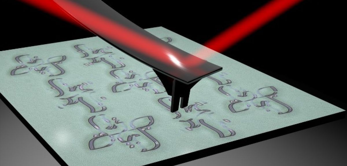
On Mark Making: An artist’s impression from inside Oxford’s Bhaskaran Lab.
Nikolaos Farmakidis invents the ‘Nanocalligraphy’ tip.
written by Méadhbh O’Connor, artist in residence.
Pressing a pen to paper, my hand travels like contours over a yet unformed topography. Spheres, globules, waves, lines and arrows emerge; rotating, floating, interacting. ‘...flipping the magnetic spins of atoms in a 2D monolayer,’ a physicist friend had been gabbling down the phone to me. Or something. His voice, converted to signals and bounced from relay to relay over a continent to me in a flash, reconfigures and amplifies out of the device into my ear.
‘...monopoles produced immediately after the big bang,’ another friend casually says in a phone call about something else.
 Méadhbh O’Connor.
 My mind drifts as the words hit my ear, meandering around spaces constructed in my head. Spinning balls, immense spaces, tiny spaces, blackness, light, no space...
‘Less like points and more like a field,’ I recall someone saying. I hold the page up in front of me with the drawing.
The marks project something back, something I don’t know consciously and can’t pin down to any singular meaning. I don’t know what it is, I don’t know what to call it and I don’t know where it came from. And yet the thoughts flowed down my arm and onto a page, like opening a valve into the mind.
To make a mark is creativity in its earliest form. From the child who, as if by instinct, reaches for the crayon to daub their first impressions, to the back of the envelope calculation that leads to a new discovery. In new technologies, the printing of a circuit board - yet another kind of mark making - has opened up the possibility for almost limitless information to be created, computed and stored on the countless gadgets that populate our world today. The mind boggles.
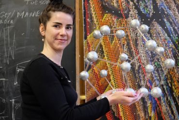
I find myself as an artist working, somehow, with a lively group of engineers at Oxford with the Advanced Nanoscale Engineering group, led by Harish Bhaskaran
Today, I find myself as an artist working, somehow, with a lively group of engineers at Oxford with the Advanced Nanoscale Engineering group, led by Harish Bhaskaran.
Wires, computers, various gadgets, gas canisters, something called an atomic force microscope, containers with tiny chips, stacks of silicon wafers, labels, tools... an abundance of odd objects are scattered around the lab. I see all this stuff and think sculpturally, ‘What could I make with this colourful wire?’
What I see is only the housing. The magic of what the group does is beyond the perception of the naked eye. One nanometer, or 100,000 times smaller than the width of a human hair, is one of the scales they use.
‘We are finding ways to capture the energy of light within nanoscale wires, while still figuring out how to make all of these sustainably and in new exotic formats,’ Professor Bhaskaran tells me.
We are finding ways to capture the energy of light within nanoscale wires, while still figuring out how to make all of these sustainably and in new exotic formats
Professor Bhaskaran
The group is busy creating a new world at this invisible scale. Lab meetings are held every other week. But we converge, instead, inside the very kind of machine their research helps to create: the computer. Transformed into pixels and in our boxes on the Zoom screen, the same questions seem to arise again and again.
‘How can we do this?’
‘What could that mean?’
‘Is there another way?’
‘Why not try this?’
Ideas dash back and forth at speed. One afternoon, I find myself in the lab talking to one or two members of the group. As expected, possibilities and ideas are being discussed with vigour. In all the enthusiastic gesticulations something flies across the room.
‘What was that?’ ‘Nothing...’
I notice the little round case that rolled across the floor with a now cracked, but thankfully unused, silicon wafer on top.
Nikolaos Farmakidis is neatly handwritten across the label. Unaware of the chaos that had just momentarily erupted in the lab, Nik is in his office concentrating fixedly at his computer, as he does every day with unyielding focus.
‘My main interests are trying to bridge optical and electrical methods for computer processing,’ he says, with a humility that belies his futuristic research.
My main interests are trying to bridge optical and electrical methods for computer processing, says Nikolaos Farmakidis. It is a bit different from my usual research. A side project...I designed a new tip for lithography at the nanoscale
He tells me of a paper he’s been working on. One of many, I note.
‘It is a bit different from my usual research. A side project,’ he modestly says.
Something unexpected, I interpret his remark.
‘I designed a new tip for lithography at the nanoscale.’
He shows me an image of an elegant circle, wide at the top and gradually narrowing at its side, and repeating again to close the infinite loop. I learn that I am seeing 100 microns, again, far smaller than the width of a single human hair. My eye darts to the right and another image is on the page, ‘My Life’ scribed beautifully in Arabic.
How better to demonstrate its potential than to consult a calligrapher, Majid Alyousef, a master of the mark. The elegant letters form an ambigram, turned upside down it cleverly reads the same. Much like Nik’s perfect circle. Nano-calligraphy he calls this novel method. Or to be more precise: Nano-Calligraphy Scanning Probe Lithography (nc-SPL). Mechanical nanolithography which can be extended to the patterning of biological materials such as proteins or DNA or even sheets, one atom thick.
A new probe to score the minutest of marks with the atomic-scale movements of the microscope it sits in. Some hobbyists even make their own such machines. It’s an inexpensive new tool for them too.
Nik and his collaborators have fashioned a new tool not just for the researcher experimenting at the frontiers of computing, but also the hobbyist, the artist and the curious to make a new mark on the world
As we stop chatting I turn back to my laptop to continue making pictures, with pixels this time, and realise how much I had taken it for granted. Every chip, screen, logic gate, the circuitry, programming language, the billions of parts, had to be thought up and made by somebody or somebodies. A humming, pulsating, electrical monument to the creativity of countless people. I stare at the device, somehow seeing it anew, and am suddenly jolted out of this distant thought. A ping leaps out of the phone, then the laptop, then the computer: a reminder with ‘Bi-weekly lab meeting’ appears on every screen.
I log in to listen in again. Never resting, the group has moved on to the next burning questions. In the meantime, Nik and his collaborators have fashioned a new tool not just for the researcher experimenting at the frontiers of computing, but also the hobbyist, the artist and the curious to make a new mark on the world.
Méadhbh O’Connor is a visual artist from Ireland who has dedicated her art practice to bringing art and science together. She is artist in residence with the Advanced Nanoscale Engineering group in the Department of Materials, University of Oxford
 25-year Oxford study finds the effects of conflict last for generations
 What Louise Thompson’s campaign tells us about the national maternity crisis
 Celebrating 25 Years of Clarendon
  Learning for peace: global governance education at Oxford
  What US intervention could mean for displaced Venezuelans
  Setting the agenda for the next century of quantum
 10 years on: The Oxford learning centre making an impact
 Mapping the Moon: the world’s first lunar atlas goes digital
  Oxford and The Brilliant Club: inspiring the next generation of scholars
 New course launched for the next generation of creative translators