New water-based approach to manufacturing semiconductors
By Yu Shu
With the increasing demand for high-tech devices such as smart phones, wearable watches and portable health monitoring devices, the semiconductor manufacturing industry faces a big challenge of fabricating these devices in a sustainable and cost-effective way.
The current semiconductor manufacturing process releases a large amount of hazardous chemical waste in the fabrication process, which poses a great threat to human beings
The current semiconductor manufacturing process releases a large amount of hazardous chemical waste in the fabrication process, which poses a great threat to human beings (e.g., toxic chemicals may contain carcinogens) and the environment (e.g., resulting in water, oil and air pollution).
Compared to chemical waste management after the production, minimisation of the use of hazardous chemicals at the source is a more effective and sustainable approach to reduce the negative impact on the environment in long term. Thus the development of a water-based manufacturing technology becomes essential to the semiconductor industry.
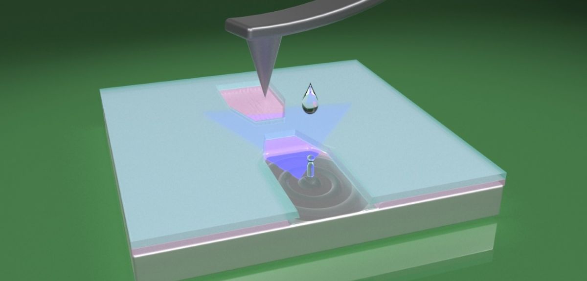
Recently we have proposed an environmentally friendly mechanical bilayer lithography approach that just uses water in the fabrication process. A nanoscale tip is employed to write patterns on the bilayer resist coated on the substrate of which one layer of resist is water soluble. This enables the water to act as the resist developer and remover and greatly reduces the use of chemicals at the source.
Recently we have proposed an environmentally friendly mechanical bilayer lithography approach that just uses water in the fabrication process
Compared to conventional photolithography techniques that use a lot of organic solvents in the fabrication process, the water-based process shows great sustainability with reduced influence of chemical wastes on the environment. Based on the fact that the key parts of smart devices are complex integrated circuits, this approach has the substantial potential to be utilised in semiconductor manufacturing as it is capable of writing various patterns in both nanoscale and microscale. The highest achievable resolution is 310 nm, with the scope of further improvement.
The water-based approach is applicable to a wide range of materials especially sensitive materials such as polymers and two-dimensional materials. This also brings a lot of opportunities in flexible and wearable technologies. Polymers with low cost, light weight and flexibility are promising flexible substrates, while two-dimensional materials that have atomic thickness and great electronic and photonic properties can be seamlessly integrated with flexible substrates.
The water-based approach is applicable to a wide range of materials especially sensitive materials such as polymers and two-dimensional materials
However, they both have the disadvantage of low resistance to chemical and radiation damage. This research gives a demonstrator of a flexible MoS2 photodetector fabricated by the water-based mechanical bilayer lithography technique. Due to the protection from chemical and radiation damage, the flexible photodetector shows a rather rapid photoresponse of 42 ms to the red laser diode with the wavelength of 633 nm, validating the superior functional applicability of the water-based process.
This research work is led by Professor Harish Bhaskaran in Department of Materials at Oxford University and is funded by EPSRC Wearable and Flexible Technologies programme. More information about the work can be found in the full paper published in Nano Letters - 'Nanoscale Bilayer Mechanical Lithography Using Water as Developer'.
Yu Shu is a DPhil student at the Department of Materials and co-authored the above paper.
About OxSciBlog
The Oxford Science Blog gives you the inside track on science at Oxford University: the projects, the people, and what's happening behind the scenes. Curated by Ruth Abrahams, Media Relations Manager (Research and Innovation).
Contact: Ruth Abrahams, [email protected]